Introduction to the wires and connectors in the DC charging...
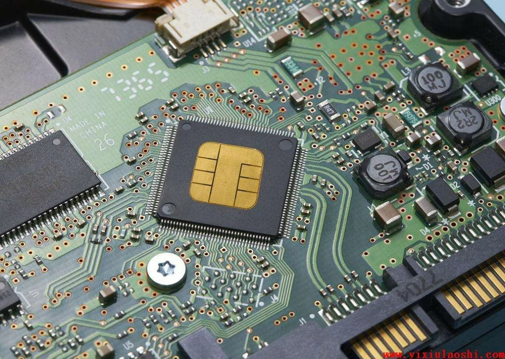
Buffer of DC charging pile communication interface chip
Main component
Concept:
The buffer of the DC charging pile communication interface chip is an electronic component mainly used to protect the power semiconductor from voltage and current transients to ensure the stability and reliability of the communication interface. Buffers reduce electromagnetic interference (EMI) by absorbing spikes in voltage and current, and provide signal integrity, which is critical to maintaining efficient and safe operation of DC charging piles.
Function:
1. Voltage and current spike absorption: The buffer can absorb voltage and current spikes caused by switching operation to protect subsequent circuits from damage.
2. Reduce electromagnetic interference: By reducing spikes and transients, buffers help reduce electromagnetic interference, which is important for meeting electromagnetic compatibility (EMC) standards.
3. Signal integrity: In the communication interface, the buffer ensures that the signal can maintain its integrity after long-distance transmission, reducing signal attenuation and distortion.
4. Hardware protection: The buffer provides hardware level protection for power semiconductors such as power MOSFETs or IGBTs to prevent damage caused by overvoltage and overcurrent.
Working Principle:
1. RC network: The buffer is usually composed of a passive RC (resistance-capacitance) network, which uses the characteristics of inductance current cannot be mutated to inhibit the current rise rate of the device, and the characteristics of capacitor voltage cannot be mutated to inhibit the voltage rise rate of the device.
2. Voltage comparator: Some buffer designs will include a voltage comparator with a specified threshold and hysteria that blocks the gate driver in case of overvoltage, thereby protecting the power semiconductor.
3. Overcurrent protection: Some buffers integrate overcurrent desaturation protection (DESAT) to reduce gate drive during overcurrent and prevent power semiconductor damage.
4. Signal conversion and isolation: In some designs, the buffer also assumes the role of signal conversion and isolation, such as the use of digital isolators to ensure the safe transmission of signals between different voltage layers or circuits.
Sum up
Through the above introduction, we can see that the buffer of the DC charging pile communication interface chip plays an important role in protecting the power semiconductor, reducing electromagnetic interference, and maintaining the integrity of the signal, and is a key component to ensure the stable operation of the DC charging pile.
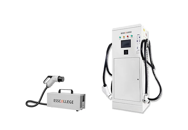
DC CHARGING PIlE SERIES
DC charging pile is an efficient charging facility for electric vehicles, which uses direct current (DC) to directly charge the vehicle battery, significantly reducing the charging time. Compared with traditional AC charging piles, DC charging piles are able to provide higher power output and can usually charge an EV to 80% of its capacity in 30 minutes, providing users with a convenient charging experience.
Extended reading
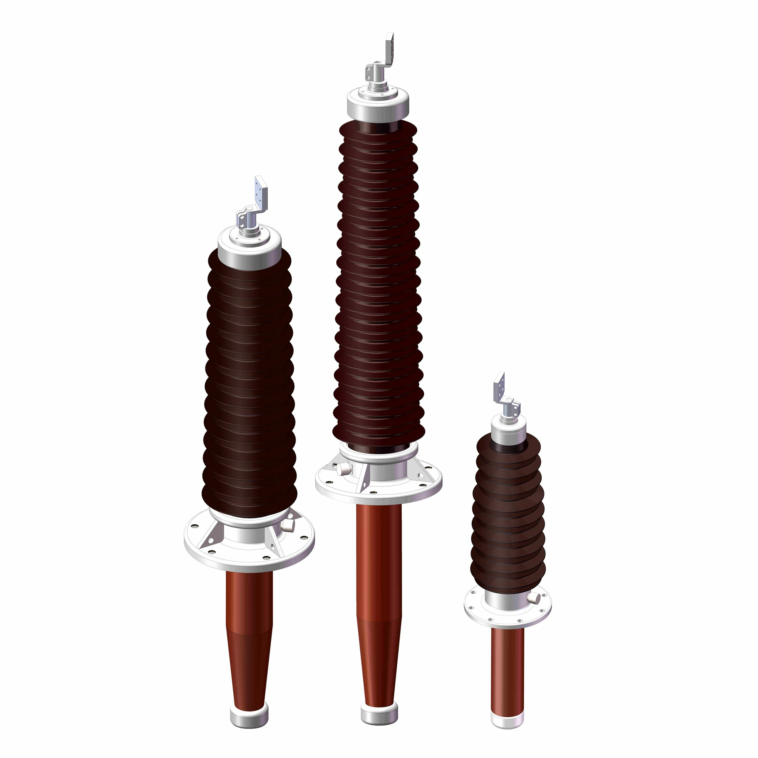
Introduction to the bushing of DC charging pile transformer
Introduction to the bushing of DC charging pile transformer The...
Introduction to the application of stainless steel plate in DC charging pile
Introduction to the application of stainless steel plate in DC...
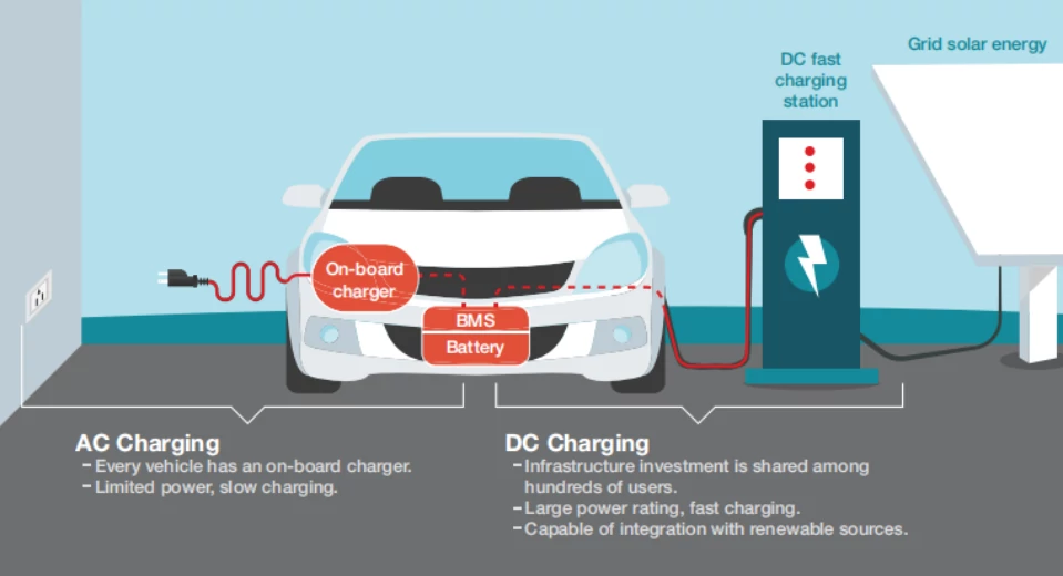
The difference between DC and AC charging pile
At present, the charging methods of electric vehicles are mainly...
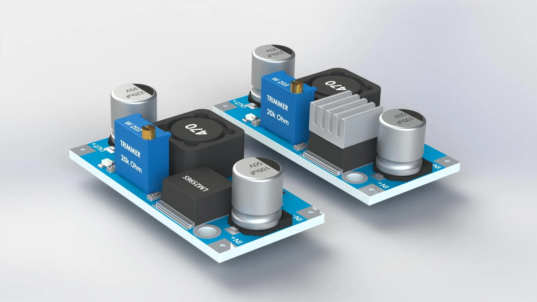
Dc charging pile display chip DC-DC converter
Dc charging pile display chip DC-DC converter Main component Concept:...
The thermal management and regulation function of DC charging pile is introduced
The thermal management and regulation function of DC charging pile...
THE ESSC Brand promise
Global supply
Our products sell well all over the world, covering many countries and regions, through the global logistics network, to provide customers with convenient purchasing experience.
Rigorous quality
We adhere to the highest quality control standards to ensure every product meets industry regulations and customer expectations, earning trust through consistent excellence.
Excellent service
With a customer-centric approach, we provide prompt responses, professional support, and personalized services, aiming to deliver the best user experience and long-term value.

